According to the latest report, the South Korean tech giant, Samsung Electronics gained the number one position as the leading investor in semiconductor capital expenditures (CAPEX) globally over the past ten years.
A reliable researcher Andrea Lati at TechInsights, announced during a press briefing at SEMICON Korea 2024 on Jan. 31 that “the semiconductor market will exhibit a robust growth rate this year, gaining positive momentum.”
Overall, DRAM and NAND Flash will see the most significant recovery, with growth rates of 50% and 32%, respectively.
Apart from the above, logic and automotive semiconductors are expected to show double-digit growth rates of 14% and 10%, respectively.
Lati said, “Last year, Samsung Electronics was the top spender in CAPEX, and it appears they will retain the top spot this year as well. Looking at the past decade, Samsung Electronics has consistently been the most significant investor in CAPEX.”

Get the latest Samsung updates on your device by joining us on WhatsApp, Telegram, Google News & X (Twitter).
Samsung Electronics is beginning to introduce hybrid bonding
Samsung is reportedly planning to start and introduce hybrid bonding to strengthen its foundry capabilities. In 2024, Besh and Applied Materials (Applied) hybrid bonding-related equipment is being set up at the Cheonan campus. The equipment is expected to be used for advanced packaging such as the next-generation X-Cube.
Reportedly, Besey and Applied are installing hybrid bonding-related equipment at Samsung Electronics’ Cheonan campus. Cheonan Campus is Samsung Electronics’ advanced packaging production base.
An industry official said, “We are currently setting up a hybrid bonding line at the Cheonan campus,” and added, “As far as I know, the equipment is used for non-memory packaging.”
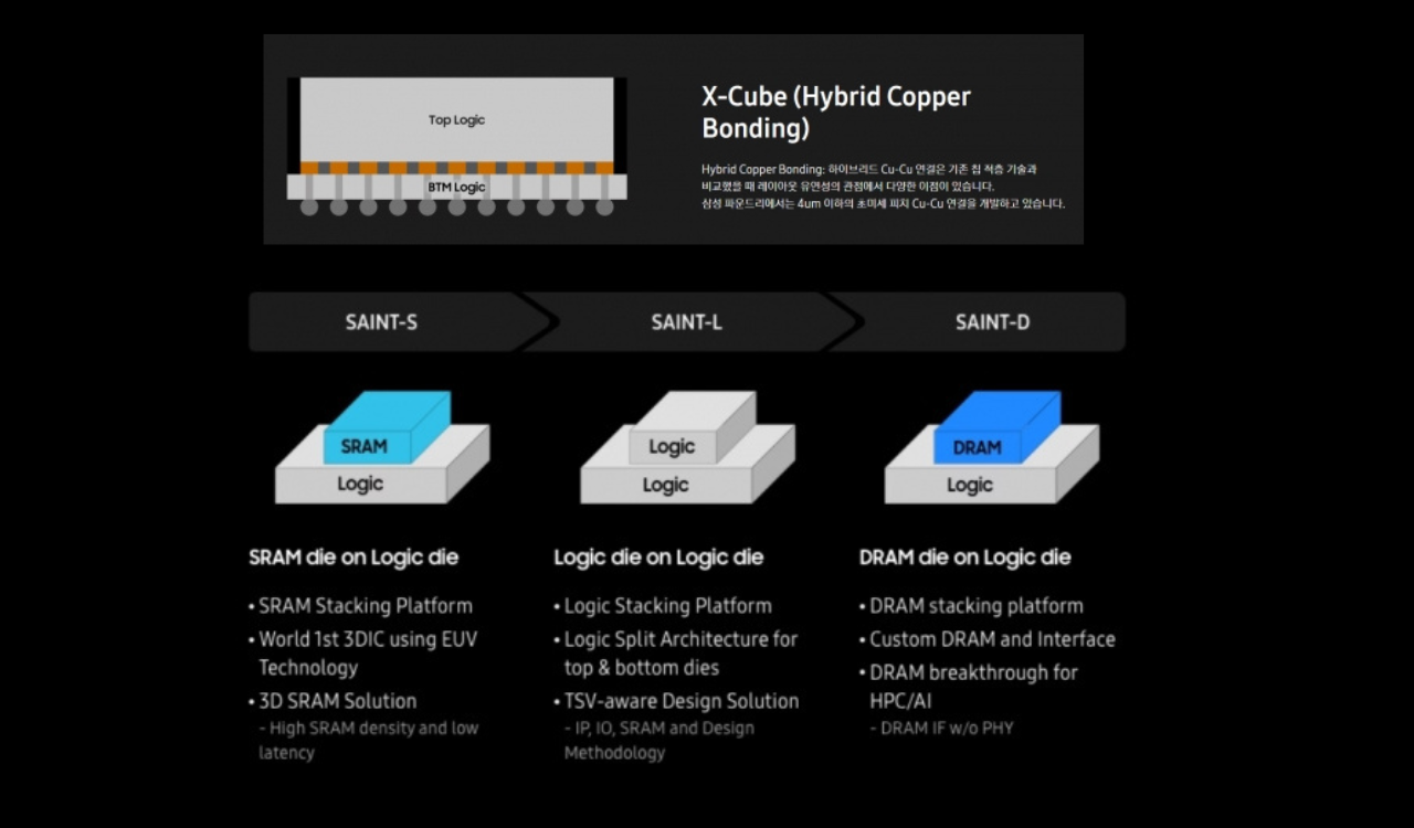
Hybrid bonding is a technology for attaching a wafer or die to a die. It has the advantage of being able to improve I/O and wiring length compared to existing bonding methods. It is known that when hybrid bonding is applied, 10,000 to 100,000 vias can be connected in an area of 1㎟. Vias are used for I/O or power supply.
Meanwhile, the South Korean tech giant is also working to introduce X-Cube using hybrid bonding. The company predicts that hybrid bonding could also be applied to the Saint platform that Samsung Electronics plans to introduce starting this year.
It plans to provide 3D packaging services such as Saint-S, which stacks SRAM on a logic die, Saint-L, which stacks logic die on a logic die, and Saint-D, which stacks DRAM die on a logic die.


