
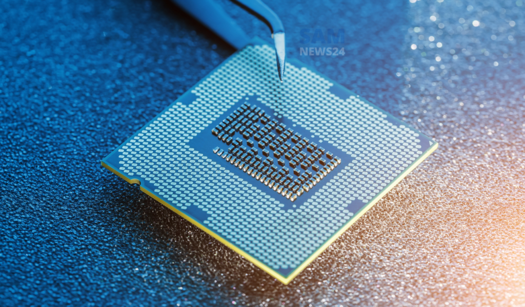
Samsung Electronics is said to be established a chip test line in Japan. Since the same info has been revealed by five people stated in Japan to strengthen its advanced packaging business. Also, subsequently, establish closer links with Japanese makers of semiconductor equipment and materials.
Notably, this would be the first test line of its kind in Japan of Samsung. Primarily, the world’s biggest maker of memory chips. This would also depict the United States’ significant desire to connect together to counter China’s increase with regard to chips and advanced technology.
In addition to this, Japan stated recently, it would prohibit the exports of 23 types of chips making tools. While implementing its technology trade controls with a U.S. push. This is intended to restrain China’s ability to make advanced chips.
Samsung is also looking to set up a facility in Kanagawa prefecture, near Tokyo. Whereby, it already has a research and development center. As stated by four people, all of them are denied to come into light since the info is not public.
However, the information is not concluded yet, including timing. On the other hand, the investment would suppose to be in tens of billions of yen, said one of the people. Japan is an attractive choice due to the low labor pricing and the existence of leading chip equipment makers. It enables Samsung to access a local “ecosystem,” revealed by another one of them.
Samsung declined to say anything
It has been also noticed that companies are competing with each other in order to generate advanced packaging techniques. The same comprises placing chips with various functions into a single package. It significantly enhances the overall capabilities and limits the additional cost of more advanced chips.
Also, the three-dimensional packaging could also help makers to improve chip performance. Notably, South Korean President Yoon Suk Yeol made their first visit to Japan this month in 12 years. This is also assumed to develop business relations with business leaders from both countries.
Since Samsung is also set up an advanced packaging team in South Korea. In particular, it is predicted to invest $230 billion over the next 20 years. This creates a large chip-making unit in the country.

FOLLOW US ON SOCIAL MEDIA – Telegram, Twitter, Facebook, & Google News.