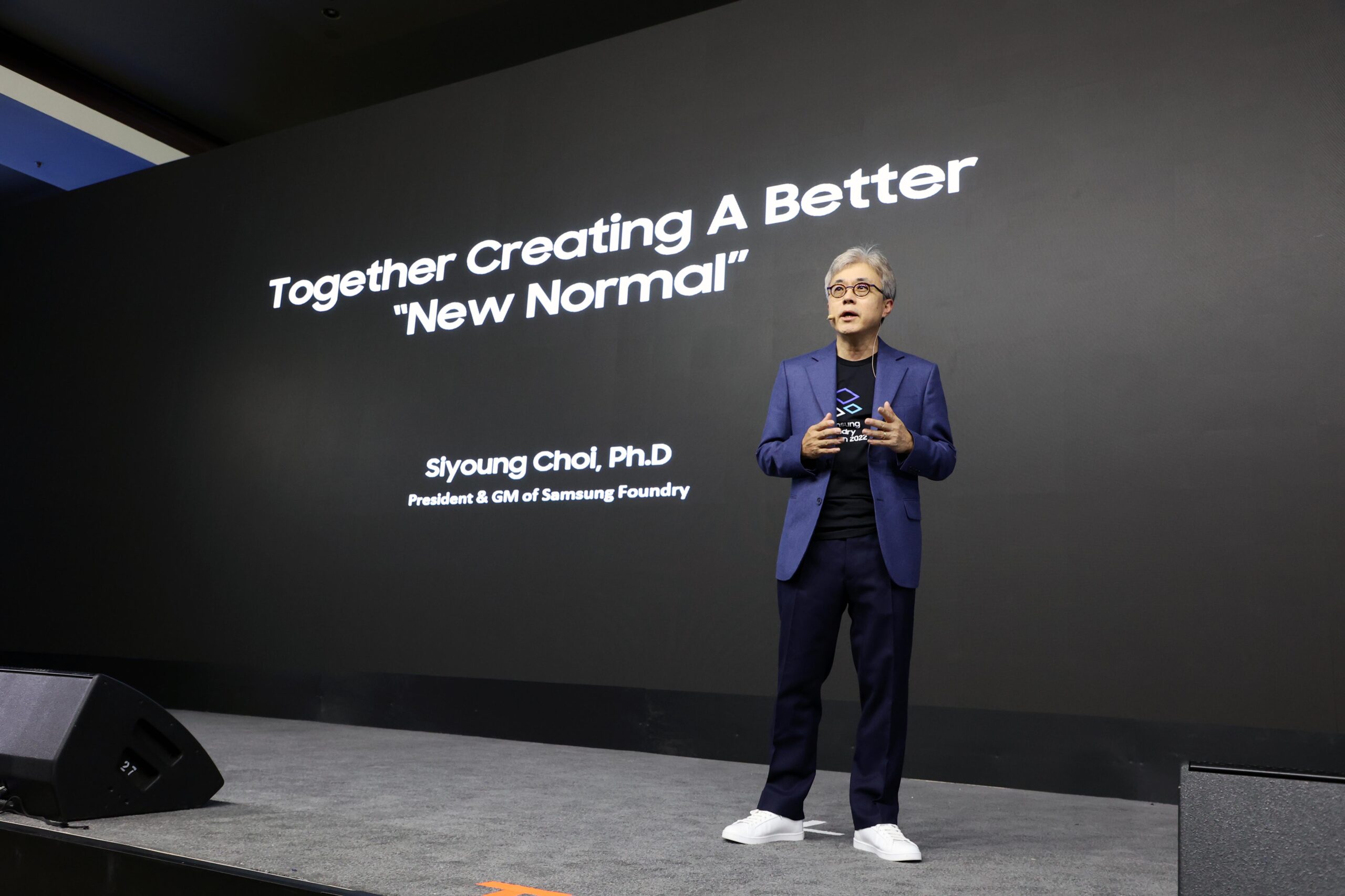
Samsung Electronics is the world’s second-biggest semiconductor chip maker firm, in order to secure the place of best-in-class foundry technology leadership. The giant announced during Samsung Foundry Forum 2022 that it going to keep on improving semiconductor chips to be smaller, faster and more energy efficient. They also plan to expand their fleet process and start to produce 2nm and 1.4nm chips respectively.
Second and third-generation 3nm GAA chips, properties of smaller transistor size and superior efficiency
Talking about Samsung’s 3nm chips then the company starts the Foundry process to produce in bulk. It is the world’s first 3nm chip (SF3E) which is based on GAA (Gate All Around) technology. Whereas GAA is an overhaul of the basic transistor design. For this, the firm commits to giving a massive improvement in power efficiency through this technology. Now, in addition to this info, the company reportedly announced a second-generation 3nm semiconductor chip (SF3) by 2024.
As per Samsung, its second generation 3nm chips are 20% smaller in size as compared to the previous one. The earlier one was first-generation 3nm chips. And it results in smaller and more energy-efficient chips being made available for smartphones, PCs, cloud servers and for wearables as well.
Additionally, the company plans to further optimise its 3nm transistor fabrication technology with its SF3P+ process. And the mass production of the same going to start by 2025. While the company has already proven its GAA chips by producing them in mass. On the other hand, its second and third-generation GAA chips will definitely attract its big lost clients. It includes Apple, AMD, Nvidia and Qualcomm, these are take over by TSMC over the past few years.
Samsung Foundry will mass produce 2nm chips in 2025 and 1.4nm chips by 2027
Meanwhile, the company also declared that it plans to initiate the making of 2nm chips by 2025. This announcement is made when the South Korean firm will adopt the backside power delivery tech for chips. As powering transistors and communicating with them is done only with the help of one side of a semiconductor chip. Also, with the new improving backside power delivery technology, the process of communication and power delivery is being subdivided into opposite sides of a chip. And as a result of this, it improves the overall chip performance. Whereas, Intel also plans to bring a similar feature (PowerVia) to its chips by 2024.
Samsung Foundry also expands a new node which is 1.4nm (SF1.4) to its semiconductor line. And the same company plans to start in mass production by 2027. Although Samsung is not disclosing yet revealed what improvements to expect from its 1.4nm chips.
Moving further, the company also improvise 2.5D/3D heterogeneous integration packaging technology. It is going to avail with micro-bump interconnection by 2024. On the other hand, bump-less 3D X-Cube will be available in 2026. The company also plans to expand chip production by more capacity, 3x by 2027 as compared to 2022.

Samsung have its focused on automotive and 5G/6G communication markets
The company expect 50% of its chip requirement may arise from automotive, High-performance computing, IoT and 5G markets. Whereas, the company will also enhance 4nm processes in order to manufacture chips for automotive and HPC domains as well. Presently, it makes 28nm eNVM chips for its automotive clients. Concurrently, it also has plans to improvise 14nm eNVM solutions in 2024, while 8nm eNVM solutions in the near future.