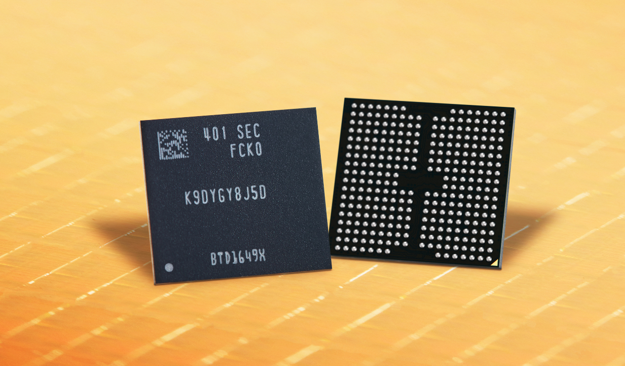
Samsung has officially started mass production for its one-terabit (Tb) triple-level cell (TLC) 9th-generation vertical NAND (V-NAND).
Here’s the official statement;
“We are excited to deliver the industry’s first 9th-gen V-NAND which will bring future applications leaps forward. In order to address the evolving needs for NAND flash solutions, Samsung has pushed the boundaries in cell architecture and operational scheme for our next-generation product,” said SungHoi Hur, Head of Flash Product & Technology of the Memory Business at Samsung Electronics. “Through our latest V-NAND, Samsung will continue to set the trend for the high-performance, high-density solid-state drive (SSD) market that meets the needs for the coming AI generation.”
The company has improved the bit density of the 9th-generation V-NAND by about 50% compared to the 8th-generation V-NAND.
In addition, Samsung’s advanced “channel hole etching” technology showcases the company’s leadership in process capabilities. This technology creates electron pathways by stacking mold layers and maximizes fabrication productivity as it enables simultaneous drilling of the industry’s highest cell layer count in a double-stack structure.
The 9th-generation V-NAND is equipped with the next-generation NAND flash interface, “Toggle 5.1,” which supports increased data input/output speeds by 33% to up to 3.2 gigabits-per-second (Gbps).
Power consumption has also been improved by 10% with advancements in low-power design, compared to the previous generation.
Get the latest Samsung updates on your device by joining us on WhatsApp, Telegram, Google News & X (Twitter).