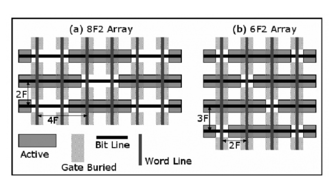
According to the information, the South Korean tech giant Samsung is developing a 4F square DRAM memory cell unit structure. The report from TheElec indicates that the chip die area can be reduced by around 30% compared to the existing 6F square class without changing the node.
Generally, 4F Square is a cell structure technology that ended in failure after the DRAM industry tried to commercialize it about 10 years ago. Samsung has now formed a team to mass-produce 4F square cell structure DRAM.
The company will develop a 4F square structure than the 3D method of stacking each DRAM element on top.
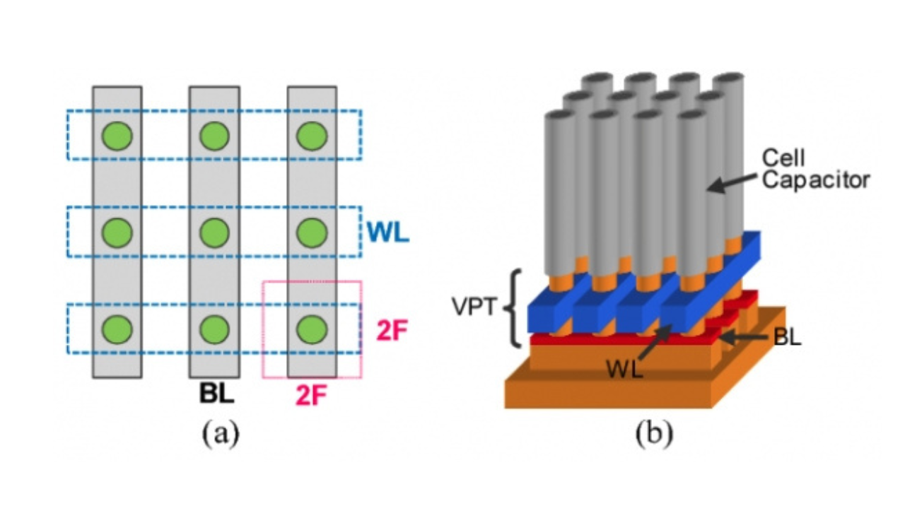

A transistor is composed of a source (S)-gate (G)-drain (D) according to the direction in which current flows in and out. Above the drain is a capacitor that stores charge. The transistor is engaged with the word line WL and the bit line BL. Since the word line is in charge of on/off switching of the transistor, it must be connected to the gate. The bit line serves to read and write data, so it is connected to the source of the transistor.