
Over a period of time, semiconductor technological advancement can be clearly observed through Gordon Moore’s famous “Moore’s Law”. “Moore’s Law” has been considered the fundamental principle of semiconductor technology development for the last five decades.
When at present technology is at its peak and smartphones hold all the possibilities in our hands. In the same era of smartphones mobile internet, AI, and big data call for increasingly faster speeds of computing performance. The mobile internet, AI, and big data call for increasingly faster speeds of computing performance. This has been occurring speed at which transistors are growing smaller to slow down. This reflects the tech is falling behind Moore’s Law.
Well, it gets increasingly difficult to maintain analog performance, and the semiconductor process becomes increasingly miniaturized. The market also demands semiconductors to be versatile, encompassing a variety of features such as analog or RF wireless communication in one chip. This smells of difficulties in meeting the demands of the market just through process miniaturization based on Moore’s Law.
In a way to find a way across the limitations of semiconductor technology, “Beyond Moore” has been in the existence beyond the prior Moore’s Law.
“Advanced Package, Leading the Beyond Moore Era”
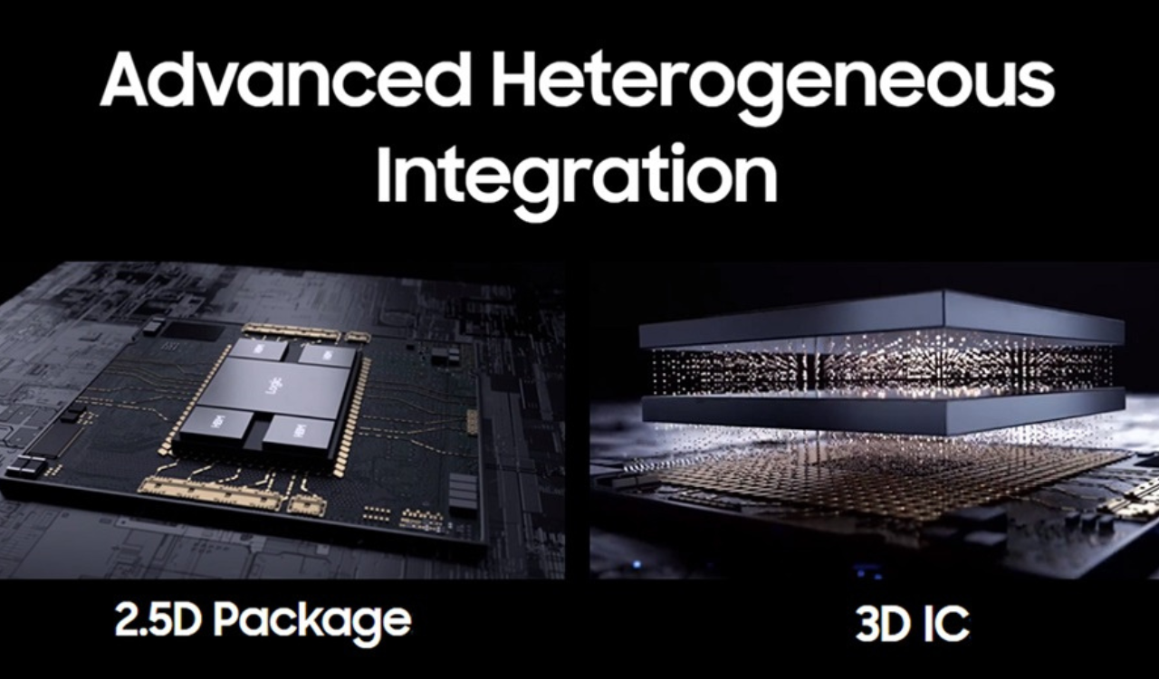
Beyond the Moore, era is Advanced Package technology through advanced Heterogeneous Integration. This can be planted with more transistors on a single chip and offers performance that is more powerful than the sum of all parts. Through connects multiple chips horizontally and vertically.

In the opinion to market research, the CAGR of the advanced packaging industry is estimated at a 9.6% growth rate between 2021 and 2027. In fact, 2.5D and 3D packages implementing heterogeneous integration are expected to show an even higher growth rate of 14%.
Governments are also paying close attention. The South Korean Ministry of Trade, Industry, and Energy hosted a forum on semiconductor packaging technology in February.
While DARPA (Defense Advanced Research Projects Agency) of the US Department of Defense announced the allocation of a large-scale budget for advanced package-related fields last April. The Japanese government also announced new incentives to attract research centers, as well as establishing a dedicated symposium.
“One-Stop Advanced Package Solution with High Performance and Low Power”
Samsung Electronics established the AVP (Advanced Package) Business Team under the Device Solutions Division last December to boost the company’s capabilities in advanced packaging technology and maximize the synergy between business units. That too in a bid to address the growing importance of advanced packaging technology.
The Korean tech giant, with industry-leading expertise in memory, logic foundry, and package business, is well-positioned to utilize heterogeneous integration to offer competitive 2.5D and 3D packages that connect state-of-the-art logic semiconductors produced with EUV and high-performance memory semiconductors such as HBM.
Focussing one-eyed development of next-generation 2.5D and 3D advanced package solutions based on RDL, Si Interposer/Bridge, and TSV stacking technologies. The AVP Business Team operates under a business model that provides one-stop advanced package solutions that enable high-performance and low-power solutions. We communicate closely and directly with customers in order to provide solutions tailored to the needs of each customer and product.
“Our Future Beyond Connection”
In a bid to address the growing importance of advanced packaging technology, Samsung Electronics established the AVP (Advanced Package) Business Team under the Device Solutions Division last December to boost the company’s capabilities in advanced packaging technology and maximize the synergy between business units.
AVP Business Team is “hyper-connection” and envisions creating a greater synergy that connects semiconductors to the world. This connects people to people and connects customers’ imaginations to reality. “Hyper-connection” is more than a simple sum of the performance and functions of each semiconductor.
However, Samsung put on its priority on the development and production strategy to fulfill its commitment to a competitive. Based on customer-oriented business development that ensures prompt responses to customer requests.
FOLLOW US ON SOCIAL MEDIA – Telegram, Twitter, Facebook, and Google News.