
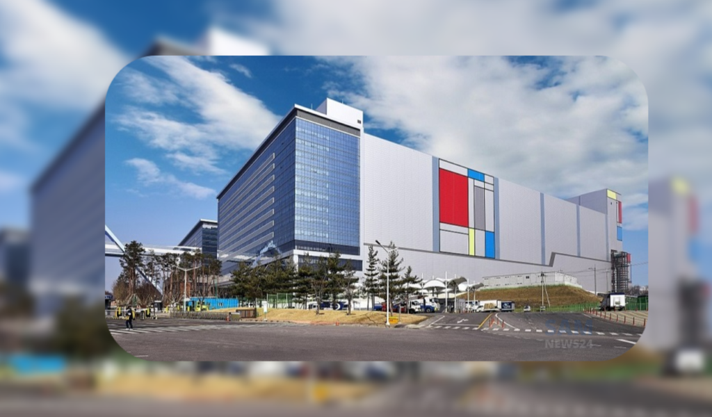
Samsung Electronics is a market leader worldwide in advanced semiconductor technology. Whereas, it has been revealed by the company that it established a Life Cycle Assessment (LCA) on the product carbon footprint of its semiconductor business. It also got verified through DNV, which is one of the world’s leading certification bodies.
While talking about LCA, then it is a methodology in order to assess environmental impacts. This is throughout the lifecycle of commercial products, processes, or services. This is achieved by quantifying the amount of energy, materials, and waste discharge. To be in more detail, with respect to its semiconductor carbon footprint. Samsung’s LCA covers raw material extraction for chip making, assembling, and testing. And their output is in accordance with ISO 14040, ISO 14044, and ISO 14067 respectively.
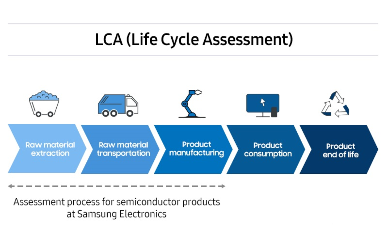

Moving ahead, the carbon footprint is used by Samsung and its customers, in order to recognize the environmental impact in all phases of Samsung’s semiconductor products. On the other hand, it is used to record and reduce carbon emissions.
“Since 2019, we have been actively mobilizing efforts to measure and reduce the carbon emissions of our key memory and logic solutions,” said Dooguen Song, Executive Vice President of the Environment, Health and Safety (EHS) Center at Samsung Electronics. “By leveraging LCA, we will be able to support our customers to achieve their carbon neutrality, as well as becoming more transparent on the environmental impact of the semiconductors we produce worldwide.”
“As a global expert in energy and environmental certification, DNV is pleased to have partnered with and to congratulate Samsung on successfully establishing its reliable LCA,” said JangSup Lee, CEO of DNV Business Assurance Korea. “Together with global business leaders like Samsung, we will continue to take part in creating a more sustainable environment in the future.”
Moving ahead with the details, then since form 2019, there are a total of 37 Samsung semiconductor products getting carbon footprint accreditation from the Carbon Trust and UL. Also, 6 of its memory products are certified for carbon reduction by Carbon Trust. Its eco-conscious product portfolio includes DRAM, SSD, embedded storage, mobile SoC, mobile Image Sensors, and automotive LED packages.
Apparently, considering sustainability at its core, Samsung will stretch its LCA, in order to include water and resource footprints. This is intended to provide a more enhanced and comprehensive assessment. It helps to decrease the environmental impact of various applications, including mobile and wearables, data centers, consumer electronics, automotive, communications, and more.