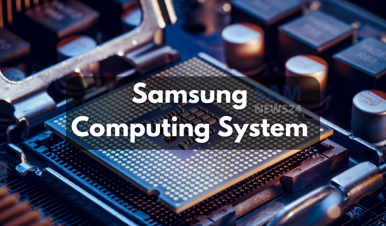
Samsung Electronics recently revealed that it has presently developed the world’s first large-scale computing system. This is achieved by connecting graphics processing units (GPUs). The same GPU has been loaded with Processing in Memory (PIM) chips. The Korean tech firm is looking for a move to share it with academia and partners.
Additionally, Vice president Choi Chang kyu, head of the AI Research Center at Samsung Electronics Advanced Institute of Technology, revealed the development of the new computing technology. They disclosed it via a keynote speech at the 2022 Artificial Intelligence (AI) Semiconductor Future Technology Conference. The conference is hosted by the Ministry of Science and ICT.
“We have built a large computing system by combining 96 GPUs (MI100) from AMD of the United States, with each of them loaded with a PIM chip. It is the only one of its kind in the world,” Choi said.
On the other hand, in October, Samsung announced that it successfully showcased the performance of processing in memory (PIM) chip by installing it on a graphics processing unit (GPU) accelerator card from AMD.
PIM is the integration of a processor with random access memory (RAM) on a single chip. Also, this technology is speculated to contribute to enhancing the performance of huge-size artificial intelligence (AI).
Also, when Samsung Electronics trained the language model algorithm T5 with this system. Their performance raised and improved by 2.5 times. While its power consumption dropped by 2.67 times as compared to PIMs are not in use.
Choi also explained the fact that the use of AI is increasing in semiconductor production processes.
“As the head of the AI research center, I want to make Samsung a semiconductor company that uses AI better than any other company,” Choi added.
As per Choi, Samsung Electronics is also researching the route in order to combine the know-how comprise in the notes of engineers working on site. By using inspection data and automatically using it in the production process.
“The current method of checking yields has its limits, as testing can only be done every three to six months when wafers are put into and taken out of the fab. We need to move on to a stage where yields can be predicted using AI sensors and inspection data,” Choi said.