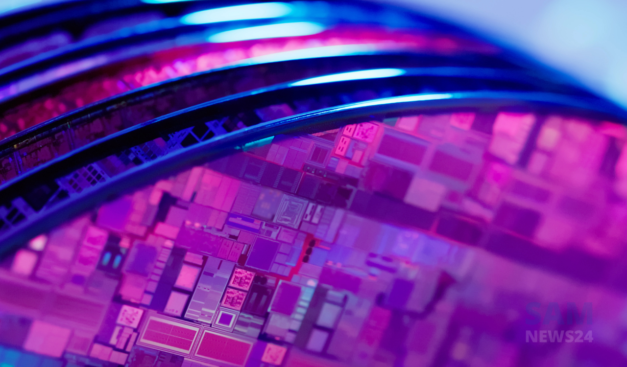
Recently, Samsung surpassed TSMC to lead in the smartphone SoC market. Samsung’s milestone done by delivering 74 million smartphones in the first three months of 2022 which is really impressive.
Another report revealed that Samsung Display will convert a few of its A3 lines to IT by the first half of 2024. Also, in 2024, a new 8.5G OLED line for IT is expected to start operating. And hence, the substrate area of Samsung Display’s IT OLED line production capacity is expected to increase from 1.38 million m² in 2022 to 2.69 million m² in 2025.
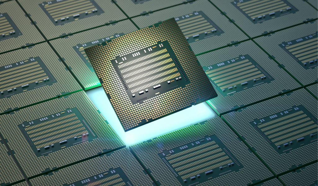
Now, the South Korean tech giant is moving up on the investment scale for the semiconductor packaging business and is evaluating an investment plan that may expand production at its Cheonan plant in South Korea.
For now, the company’s semiconductor packaging capacity is situated in Wenyang and Cheonan, Chungcheongnam-do, South Korea. Talking about the R&D center, the company has its place in Suzhou. At present, Samsung may be renting the space of the Samsung Display Tianan factory, a subsidiary of the group, to expand production.
To increase the scale in the packaging field, Samsung Electronics DS department established a semiconductor packaging task force (TF) in mid-June, which consists of DS department test and system packaging (TSP) engineers, semiconductor It consists of researchers at the R&D Center, and the head of the company’s memory and wafer.